L21: Latches#
Let’s practice Boolean algebra!
Objective
Practice usage of theorems 5-17 of Boolean algebra.
Before the Lecture#
Required Textbook Reading:
- 5.1 – 5.3 (Latches)
Basic Latch#
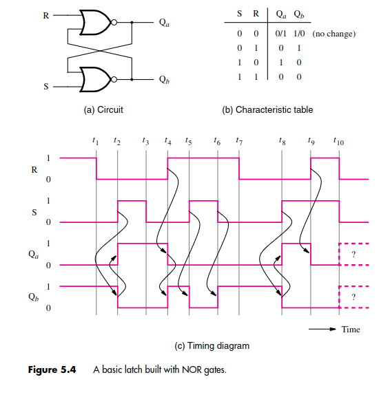
A basic latch is a memory element built from cross-coupled NOR gates with Set and Reset inputs that control the output state Q. When both inputs are 0, the latch maintains its current state due to feedback. The outputs Qa and Qb are normally complementary. When R=1 and S=0, the latch resets to Qa=0 and Qb=1. When R=0 and S=1, it sets to Qa=1 and Qb=0. When R=S=1, both outputs go to 0, creating an indeterminate state. The behavior is described by a characteristic table (rather than a truth table) because outputs depend on previous states. A timing diagram shows how state changes propagate through the gates. When both R and S transition from 1 to 0 simultaneously, oscillation can occur between states due to gate delays, ultimately settling into one stable state unpredictably.
Gated SR Latch#
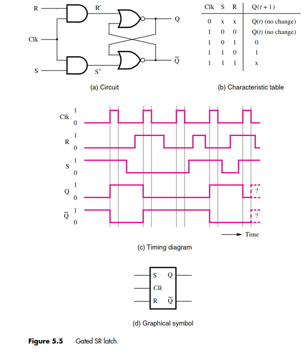
A gated SR latch adds a control signal (Clk) to the basic SR latch using AND gates. When Clk = 0, the latch maintains its state regardless of S and R inputs. When Clk = 1, it behaves as the basic SR latch—setting when S = 1, resetting when R = 1. The state Q(t+1) depends on the Clk signal and input values. When both S = R = 1, the next state is undefined. A timing diagram shows Clk as a periodic signal controlling when state changes can occur. This gated approach allows state changes only at well-defined time intervals, useful in digital systems where synchronous operation is needed. To ensure proper operation, avoid having both S and R equal to 1 when Clk transitions from 1 to 0, as this causes unpredictable behavior.
Gated D Latch#
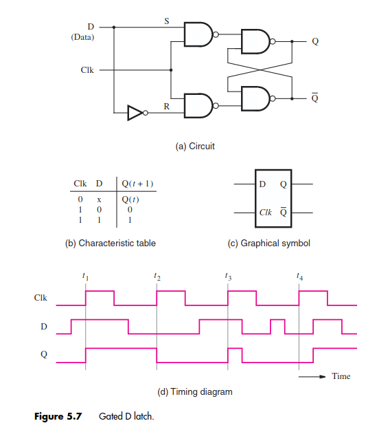
A gated D latch simplifies the SR latch by using a single data input (D) and a clock signal (Clk). The D input is connected to the S input of the SR latch, while the inverted D input is connected to the R input. When Clk = 1, the latch captures the value of D and holds it at Q. When Clk = 0, the latch maintains its previous state regardless of D. This design eliminates the indeterminate state present in SR latches when both inputs are high. A timing diagram illustrates how Q follows D when Clk is high and retains its value when Clk is low, making it suitable for storing binary information in digital circuits.