Lab8: Decoding & Encoding
Time Estimate2-4 Hours Grade Impact2.5% DueNov 11 @ 3pm Required for Pass
Objective
Reinforce modular design techniques with multiplexers and decoders – design a 2-digit seven segment display.
Warning
Before starting any lab, always read the entire lab description. You are working with expensive, fragile hardware. Look particularly closely at these boxes, which warn you of potential problems.
Before the Lab
Repository
Fork your Lab7 repository or create a new repository for this assignment, whichever you prefer. Add your instructor and TA as collaborators.
Equipment
Please bring the following equipment to this lab:
- Digilent Basys 3 FPGA board
- Compatible (power-and-data) USB cable
- Note taking mechanism (laptop, notebook, etc.)
Pre-Lab Work
This lab has pre-lab work, specified below. Pre-lab work is due within the first 30 minutes of the lab session designated for this lab (that is, 3:00pm on October 14).
Pre-Lab
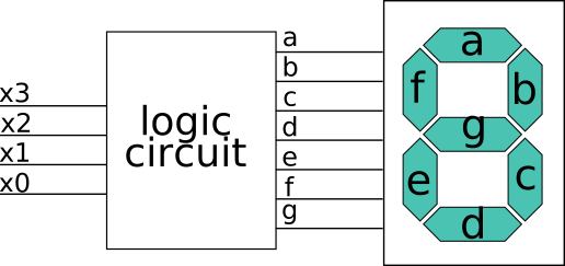
Examine the truth table you created for the seven-segment display driver (copied below). For each column a, b, . . . ,
g, convert vertically from 16 binary digits to 4 hexadecimal digits. In each group of four digits,
consider the top bit to be the MSB. In other words, for every column the input value 0 will be the
MSB and 15 will be the LSB. For example, column a should yield 16'b1011011111101011, or 16'xB7EB
Clock Division
The Basys3 board has a clock signal, clk, with a frequency of $100\ \text{MHz}$, or $100 \times 10^6\ \text{Hz}$.
The period $T$ and frequency $f$ of a signal are related by:
$$T = \frac{1}{f}$$
Therefore, the clock period is:
$$T = \frac{1}{100 \times 10^6} = 10^{-8}\ \text{s} = 10^{-5}\ \text{ms}$$
We want to refresh two display units so that only one is active at a time, with each display active for exactly $0.5\ \text{ms}$. A single signal can control the displays: when the signal is high, the first display is on; when it is low, the second display is on. This can be implemented using the clock divider developed in previous labs.
For each display to be on for $0.5\ \text{ms}$, the clock divider’s output signal must have a period of $1\ \text{ms}$. Thus, its frequency should be:
$$f_{\text{out}} = \frac{1}{1\ \text{ms}} = 1\ \text{kHz}$$
The Basys3 board’s clock frequency is $f_{\text{in}} = 100\ \text{MHz}$. Using the clock-divider formula from Lab 2,
$$f_{\text{out}} = \frac{f_{\text{in}}}{2N}$$
solve for $N$.
Verilog hint
Distinguish the divider’s toggle interval from the output’s full period. The output changes state after everyNinput cycles, so it takes two toggle intervals to return to its starting state.
Deliverable Checkpoint
Submit your pre-lab work (on Canvas or in-person).
In the Lab
Use the module names and port names below, or document equivalent names in your source. Use named port connections when instantiating modules. Simulate each module before using it in a larger design.
You have likely completed a good deal of this work in the previous lab. Reuse any modules you can to save time and effort.
The Basys3 board allows us to define only one seven-segment display digit at a time, but there are four digits on the board. In previous labs, you were able to display the same value on all digits. How can we display separate values on all four digits at the same time? The answer has to do with persistence of vision, which is the basic idea behind almost all display hardware. A digital system is able to scan through an array of displays much faster than the human eye can perceive. If we rapidly display one digit, then the next, then the next, and so on, our eyes will perceive it as a simultaneous display. If the display is updated too slowly, then the eye will perceive the scanning process. If it is done too rapidly, then the display drivers will not have time to fully illuminate the digits and they will look dim or off. So we will need to design a system with precise timing that carries out these steps:
- Select data for digit 0, decode segments, and activate anode 0
- Select data for digit 1, decode segments, and activate anode 1
- Repeat these steps indefinitely
To achieve this, our top-level design will look like the circuit diagram in the figure below.
3-to-8 decoder
Create decoder3_8.v with:
- Input
d[2:0] - Input
en - Output
o[7:0]
When en is low, every output must be zero. When en is high, exactly one output must be high: o[d].
Verilog hint: output indexing
The stated behavior iso[d] = 1when enabled. For example, address3'b101selectso[5]. Be consistent about this bit ordering in the 4-to-16 decoder and your testbench.
2-to-1 MUX
Create or reuse your MUX with inputs i[1:0], sel, and output o. Its behavior is:
sel == 0:o = i[0]sel == 1:o = i[1]
Test all eight combinations of the two data inputs and select input.
Verilog hint
The conditional operatorsel ? i[1] : i[0]can describe the MUX. If you use a different port order or names than your previous Lab7 MUX, adapt your instantiations accordingly.
4-to-16 decoder
Create a structural design using two instances of your 3-to-8 decoder to build a 4-to-16 decoder. Use internal wires for the smaller decoder enable signals. Connect the two output vectors to o[7:0] and o[15:8].
Simulate all 32 combinations of en and d[3:0]. Verify:
- Disabled means all outputs are zero.
- Enabled means exactly one output is high.
- The active output index equals the four-bit address.
Verilog hint: structural wiring
Declare internal enable signals aswire, then drive them withassignstatements. A module output connected to a slice such aso[7:0]must have the same width as that slice.
Parameterized MUX array
Create a module MUXarrary that selects between two buses:
- Parameter
SIZE, default value4 - Inputs
a[SIZE-1:0],b[SIZE-1:0], andsel - Output
o[SIZE-1:0]
Construct the array using a generate loop containing one 2-to-1 MUX instance per bit. Verify it with at least two sizes, including the default size and a different size such as 8.
Verilog hint:
generate
Declare agenvar, use aforloop inside agenerateblock, and give the loop a name afterbegin:. In each iteration, connect bitifrom both input buses to one MUX and bitiof the output bus to that MUX’s output.
Verilog hint: parameter override
The default parameter can be used by instantiating the module normally. To test another width, override it with syntax such asMUXarray #(.SIZE(8)). Ensure the connected signals are also 8 bits wide.
Truth-table exercise in Verilog
Implement the pre-lab function using your 3-to-8 decoder and OR gates. Use one decoder instance with en asserted. Express x and y as ORs of the decoder output lines identified in your pre-lab.
Simulate every input combination and compare the outputs to the truth table.
Verilog hint: reduction operators
The reduction OR operator|combines every bit of a vector into one bit. The bitwise AND operator&operates bit by bit between same-width vectors. These operators are different from logical||and&&; select the operator that matches the widths and behavior you intend.
Deliverable Checkpoint
Demonstrate a working testbench, explaining why the design is working.
Seven-segment decoder
Create module DecodedSevenSegment with a 4-bit hexadecimal input and a 7-bit segment output. Instantiate a 4-to-16 decoder with its enable asserted. Use the seven pre-lab hexadecimal masks to select the truth-table row and calculate each segment output.
For each segment, your design should:
- Combine the decoder output vector with that segment’s mask using bitwise AND.
- Reduce the resulting vector to one bit using reduction OR.
The seven output bits should represent segments a through g. Keep this module active-high internally, then handle the Basys 3 active-low polarity at the top level.
Verilog hint: select one truth-table row
A decoder produces a one-hot vector. ANDing it with a segment mask leaves a1only if the selected input’s row turns that segment on. Reduction OR converts that vector to the single segment result. Use a 16-bit mask for each segment.
Compare against the reference design
You have created a working seven-segment module. Let’s use it as a reference to simplify the testing of the new module. Copy it into this project and make its interface match DecodedSevenSegment (one 4-bit input and one 7-bit output).
Create a testbench that drives all 16 input values to both modules. Compute the bitwise XOR of their outputs, then use reduction OR to produce a single not_the_same signal. It should remain low for every input.
Verilog hint: equivalence check
Iferr = segNew ^ segReference, thenerris zero only when every corresponding segment bit matches.|erris high if any output bit differs. Make sure the two instances receive the same input and compare signals in the same bit order and polarity.
Deliverable Checkpoint
Demonstrate a working testbench, explaining why the design is working.
Two-digit seven-segment display
Create a structural top-level module named DoubleSevenSegment. It must use:
- A clock divider
- Your
MUXarray - Your
DecodedSevenSegment
Use the top four switches for one hexadecimal digit and the bottom four switches for the other. The divider output is the digit-select signal. The MUX array selects one of the two 4-bit switch values, and the selected value is decoded to seven segments.
Use the divider value calculated in the pre-lab. Drive the two used anodes so that only one digit is active at a time. Set unused anodes high so the unused digits remain off. Invert the active-high segment outputs when driving the Basys 3 segment pins.
Verilog hint: anode selection
Many Basys 3 signals are active-low. If yourselectsignal is high for one digit, that digit’s anode must be driven low and the other digit’s anode high. Check the board’s digit numbering and your constraints file rather than relying on assumed values.
Verilog hint: reuse the divider parameter
GiveDoubleSevenSegmentaPRESCALERparameter and pass it to theClockDividerinstance. In the board build, use the pre-lab value. In the simulation, override it with a small value such as 8 so you can observe digit switching without simulating a long interval.
Create a testbench for DoubleSevenSegment. Use a small divider parameter (e.g., 3) and test:
- The selected digit alternates.
- The corresponding anode is enabled while the other used anode is disabled.
- The segment outputs represent the selected switch nibble.
- Unused anodes remain off.
Deliverable Checkpoint
Demonstrate a working testbench, explaining why the design is working.
Program the Basys 3 and demonstrate that the two digits display separate hexadecimal values. Test all values from 0 through F on both digits.
Aha moment
The digits are not actually illuminated simultaneously. The design rapidly switches between them; persistence of vision makes them appear continuously lit. Try a much slower divider value in simulation and observe how the display selection changes over time.
Deliverable Checkpoint
Demonstrate a working implementation, explaining why the design is working.
Deliverables
Indicate to your instructor that you’re ready to submit your work by leaving a comment on the Feedback PR and requesting a review from @mossbiscuits. Ensure that your submission is on the main branch. Create a tag named done to mark your submission:
git tag -a done -m "Lab8 submission"
git push origin done
If you took photos, screenshots, or videos, remember to upload them to Box or OneDrive and link to them in the Feedback PR. Alternatively, you can submit these items directly on Canvas.
To receive 100 points, submissions must include evidence of the following:
- (20) Correct and timely completion of the pre-lab work
- (20) Seven-segment with Decoder simulation
- (30) Double seven segment simulation
- (30) Double seven segment implementation